
Nanoquakes Probe New 2-Dimensional Material
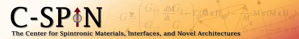
 Schematic representation of hybrid device and
 operation in surface acoustic and transistor mode.
Image copyright Hubert Krenner (Univ. Augsburg)
& Ludwig Bartels (UC Riverside
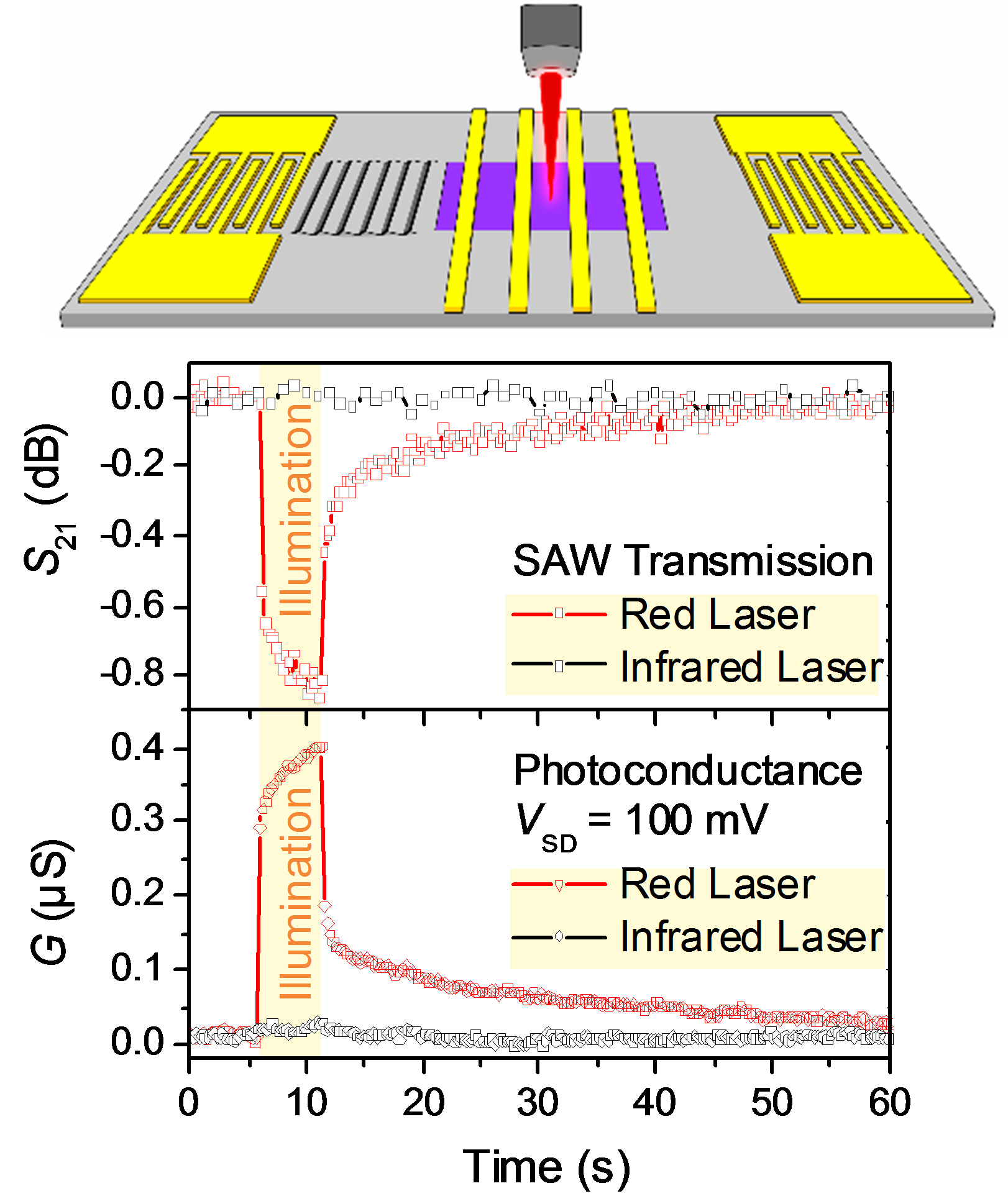
A collaboration of students and researchers from the Universities of Augsburg (Germany) and California-Riverside (USA) has devised a novel hybrid device capable of elucidating the properties of 2-dimensional transition metal chalcogenides, a key ingredient of the post-graphene era in new materials for electronic applications. Reporting in the Oct. 23rd issue of Nature Communications, they show that the fabrication of surface acoustic waves, nanometer-scale tremors of a crystalline surface following physical laws much akin to earthquakes, can sense the presence of charge carriers in a whole class of new materials. For instance, they show that shining a laser spot on a tiny micrometer-scale spot on these materials can be sensed by these waves from millimeter afar without the need for any contacts applied to the new material.
The surface acoustic waves (SAWs) at the foundation of their experiments have been used widely from frequency filters in cell-phones to mixing of solutions in tiny biomedical devices. The well-established nature of the substrates and processes to create these waves makes the novel technique facile and ready to be applied. In particular, even remote, wireless sensing applications appears to be within reach.
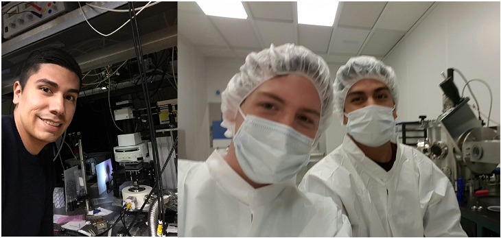 UCR student Edwin Preciado working at Augsburg Univ. and
 Augsburg student Sebastian Hammer working with Edwin
at UC Riverside. Image copyright Hubert Krenner
(Univ. Augsburg) & Ludwig Bartels (UC Riverside
This project involved students from both locations. “For this project we massively benefited from our complementary expertise. Their unique combination really allows us to open new perspectives.”, Ludwig Bartels notes. Material fabrication proceeded at the University of California followed by device integration in Bavaria. Hubert Krenner, who is also a member of the German Cluster of Excellence Nanosystems Initiative Munich (NIM) adds: “It was really exciting to see how our students obtained these fascinating results by combining the 2D materials from California and our expertise in surface acoustic waves.” UC-Riverside student Edwin Preciado and Univ. of Augsburg recent graduate Florian Schülein spear-headed this research project in the research laboratories of Ludwig Bartels (UC Riverside) and of Hubert Krenner at the chair of SAW-pioneer Achim Wixforth (Augsburg), respectively. “International collaboration and the possibility to travel to Germany was crucial for the success of this project” says Edwin Preciado. “I learned very much staying for a few months in Augsburg and it provided me with experience and skills that otherwise I would not have been able to acquire”. Likewise, a student from Augsburg (Sebastian Hammer) spent time this summer at UC-Riverside working on an extension of the current project toward the control of optical devices.
This project was supported by C-SPIN, a STARnet center of the Semiconductor Research Corporation, the National Science Foundation of the United States, the Deutsche Forschungsgemeinschaft and the Cluster of Excellence “Nanosystems Initiative Munich” (NIM) in Germany. The collaborative interaction was facilitated by generous support from the Bavaria-California Technology Center (BaCaTeC).
